Embed Size (px)
Citation preview
WAFER BONDING TECHNOLOGY
Toya Amechi Dept. of Electrical and Computer Engineering Georgia Institute of Technology, Atlanta, GA.
INTRODUCTION
Wafer bonding is a process that joins, temporarily or permanently two wafers or substrates using a suitable technology. Importance • To make silicon-on-insulator (SOI) wafers • To create complex 3D structures • Used in packaging to create closed environments • Integration technology for joining two chips fabricated
separately (CMOS+MEMS) Paper Objective To discuss the different technologies used in wafer bonding, the possible areas of application, operational conditions and pros and cons.

CLASSIFICATION

TECHNOLOGIES• Direct bonding is the joining of mirror-polished
semiconductor wafers without the use of an adhesive.
• Anodic bonding involves bonding of semiconductor wafers at slightly elevated temperature using the assistance of a strong electrostatic field.
• Thermocompression bonding involves the use of metals like Au, Cu and Al as intermediate layers in the bonding process, depending on inter-diffusion of the metallic atoms at elevated temperature with applied force.
• Eutectic bonding is a bonding technique using an intermediate metal layer that can produce a eutectic system.
• Glass frit bonding involves the use of glass as an intermediate layer in the bonding process. The glass is heated until it completely wets the surfaces to be bonded, creating a sealing bond.
• Adhesive bonding makes use of an intermediate polymer layer to create a bond between two surfaces.
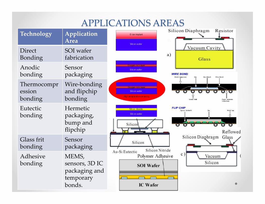
APPLICATIONS AREASTechnology Application
AreaDirect Bonding
SOI wafer fabrication
Anodic bonding
Sensor packaging
Thermocompression bonding
Wire-bonding and flipchip bonding
Eutectic bonding
Hermetic packaging, bump and flipchip
Glass frit bonding
Sensor packaging
Adhesive bonding
MEMS, sensors, 3D IC packaging and temporary bonds.

COMPARISONTechnology Typical Bonding conditions Advantages and Disadvantages
Direct bonding 600-1200CSmall to no applied pressure
+strong bond, hermetic, resistant to high temperature.-high surface flatness required, high bond temperature, bad for electronics.
Anodic bonding 150-500C200-1500VNo bonding pressure
+strong bond, hermetic, resistant to high temperature.-high temp. with high voltage, not good for electronics.
Thermocompression bonding 350-600C100-800MPa (high bond pressure)
+hermetic, compatible with electronic wafers.-very high force and high flatness required.
Eutectic bonding 200-400CLow to moderate bond pressure
+strong bond, hermetic, compatible with electronics.-sensitive to surface oxide.
Glass frit bonding 400-1100CLow to moderate bond pressure
+strong bond, hermetic.-high temperature not good for electronic wafers.
Adhesive bonding Room Temp.-400CLow to moderate bond pressure
+strong bond, low temp. works with any substrate material.-not hermetic, limited temperature stability.
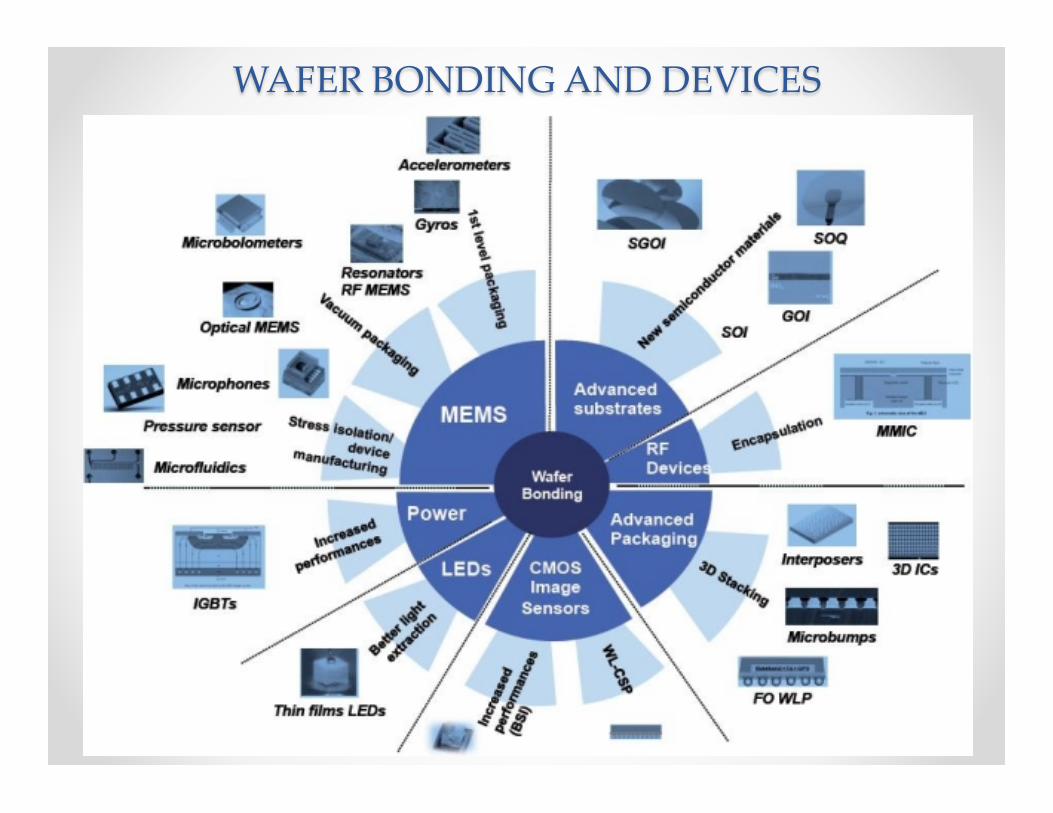
WAFER BONDING AND DEVICES
CONCLUSION
The different wafer bonding technologies find their uses in different areas of microelectronics fabrication and packaging, depending on the requirements and materials to be bonded. While the technologies are functional, further research is being carried out on various ways to improve on the already existing technologies.