Embed Size (px)
Citation preview
7/30/2019 FGA20S125P
http://slidepdf.com/reader/full/fga20s125p 1/8
© 2012 Fairchild Semiconductor Corporation 1 www.fairchildsemi.com
FGA20S125P Rev. C3
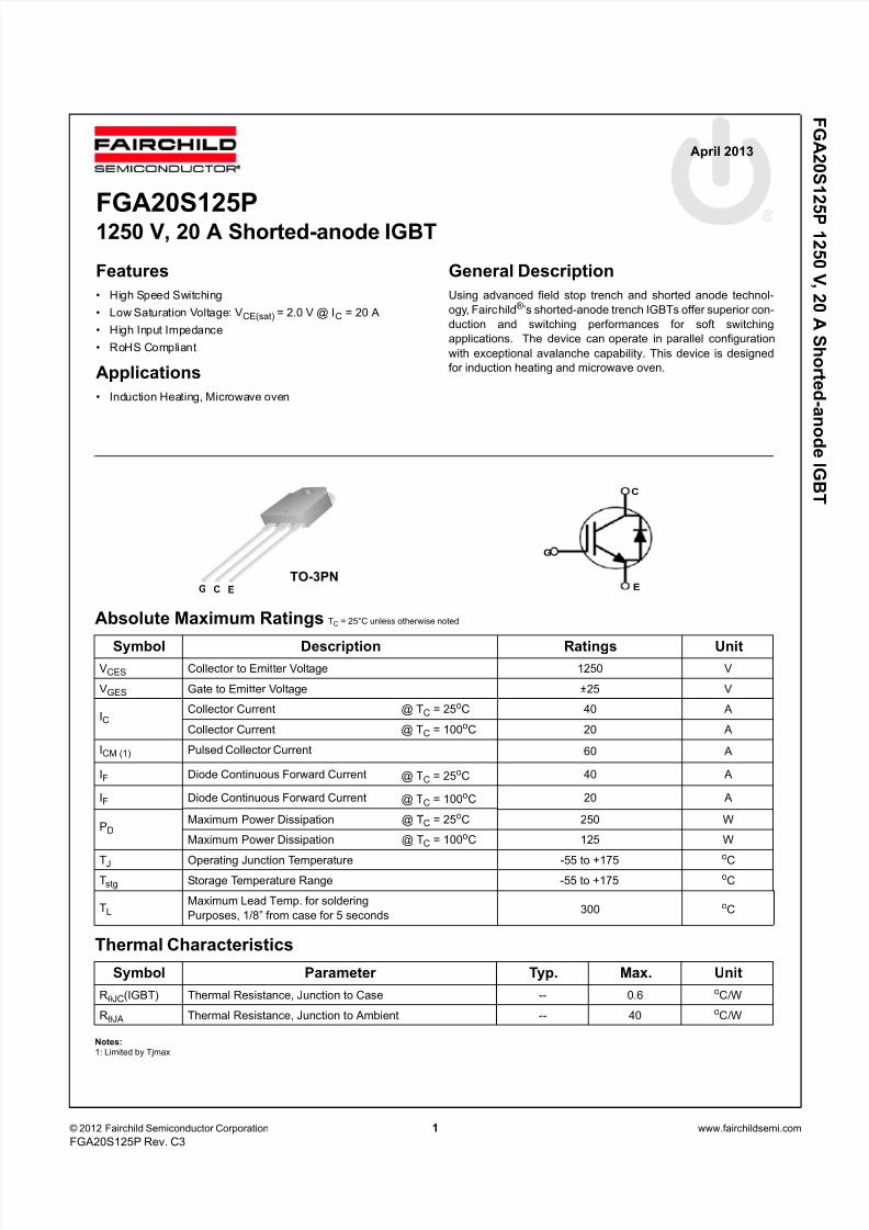
April 2013
F GA2 0 S 1 2
5 P 1 2 5 0 V ,2 0 A S h or t e d - an o d eI GBT
Absolute Maximum Ratings TC = 25°C unless otherwise noted
Thermal Characteristics
Notes:1: Limited by Tjmax
Symbol Description Ratings UnitVCES Collector to Emitter Voltage 1250 V
VGES Gate to Emitter Voltage ±25 V
ICCollector Current @ TC = 25oC 40 A
Collector Current @ TC = 100oC 20 A
ICM (1) Pulsed Collector Current 60 A
IF Diode Continuous Forward Current @ TC = 25oC 40 A
IF Diode Continuous Forward Current @ TC = 100oC 20 A
PDMaximum Power Dissipation @ TC = 25oC 250 W
Maximum Power Dissipation @ TC = 100oC 125 W
TJ Operating Junction Temperature -55 to +175o
CTstg Storage Temperature Range -55 to +175 oC
TLMaximum Lead Temp. for soldering
Purposes, 1/8” from case for 5 seconds300 oC
Symbol Parameter Typ. Max. Unit
RθJC(IGBT) Thermal Resistance, Junction to Case -- 0.6 oC / W
RθJA Thermal Resistance, Junction to Ambient -- 40 oC / W
G C E
TO-3PN
G
C
E
FGA20S125P1250 V, 20 A Shorted-anode IGBT
Features
• High Speed Switching
• Low Saturation Voltage: VCE(sat) = 2.0 V @ IC = 20 A
• High Input Impedance
• RoHS Compliant
Applications
• Induction Heating, Microwave oven
General Description
Using advanced field stop trench and shorted anode technol-
ogy, Fairchild®’s shorted-anode trench IGBTs offer superior con-
duction and switching performances for soft switching
applications. The device can operate in parallel configuration
with exceptional avalanche capability. This device is designed
for induction heating and microwave oven.
7/30/2019 FGA20S125P
http://slidepdf.com/reader/full/fga20s125p 2/8
F GA2 0 S 1 2 5 P 1 2 5 0 V ,2 0 A S h or t e d - an
o d eI GBT
© 2012 Fairchild Semiconductor Corporation 2 www.fairchildsemi.com
FGA20S125P Rev. C3
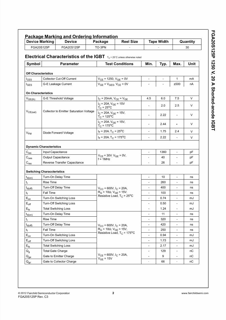
Package Marking and Ordering Information
Electrical Characteristics of the IGBT TC = 25°C unless otherwise noted
Device Marking Device Package Reel Size Tape Width Quantity
FGA20S125P FGA20S125P TO-3PN - - 30
Symbol Parameter Test Conditions Min. Typ. Max. Unit
Off Characteristics
ICES Collector Cut-Off Current VCE = 1250, VGE = 0V - - 1 mA
IGES G-E Leakage Current VGE = VGES, VCE = 0V - - ±500 nA
On Characteristics
VGE(th) G-E Threshold Voltage IC = 20mA, VCE = VGE 4.5 6.0 7.5 V
VCE(sat) Collector to Emitter Saturation Voltage
IC = 20A, VGE = 15V
TC = 25oC- 2.0 2.5 V
IC = 20A, VGE = 15V,TC = 125oC
- 2.22 - V
IC = 20A, VGE = 15V,
TC = 175oC- 2.44
-
V
VFM Diode Forward VoltageIF = 20A, TC = 25oC - 1.75 2.4 V
IF = 20A, TC = 175oC - 2.22 - V
Dynamic Characteristics
Cies Input CapacitanceVCE = 30V, VGE = 0V,
f = 1MHz
- 1360 - pF
Coes Output Capacitance - 40 - pF
Cres Reverse Transfer Capacitance - 26 - pF
Switching Characcteristics
td(on) Turn-On Delay Time
VCC = 600V, IC = 20A,
RG = 10Ω, VGE = 15V,
Resistive Load, TC = 25oC
- 10 - ns
tr Rise Time - 260 - ns
td(off) Turn-Off Delay Time - 400 - ns
tf Fall Time - 100 - ns
Eon Turn-On Switching Loss - 0.74 - mJ
Eoff Turn-Off Switching Loss - 0.50 - mJ
Ets Total Switching Loss - 1.24 - mJ
td(on) Turn-On Delay Time
VCC = 600V, IC = 20A,RG = 10Ω, VGE = 15V,
Resistive Load, TC = 175oC
- 11 - ns
tr Rise Time - 320 - ns
td(off) Turn-Off Delay Time - 420 - ns
tf Fall Time - 250 - ns
Eon Turn-On Switching Loss - 0.94 - mJ
Eoff Turn-Off Switching Loss - 1.23 - mJ
Ets Total Switching Loss - 2.17 - mJ
Qg Total Gate Charge
VCE = 600V, IC = 20A,
VGE = 15V
- 129 - nC
Qge Gate to Emitter Charge - 9 - nC
Qgc Gate to Collector Charge - 66 - nC
7/30/2019 FGA20S125P
http://slidepdf.com/reader/full/fga20s125p 3/8
F GA2 0 S 1 2 5 P 1 2 5 0 V ,2 0 A S h or t e d - an
o d eI GBT
© 2012 Fairchild Semiconductor Corporation 3 www.fairchildsemi.com
FGA20S125P Rev. C3
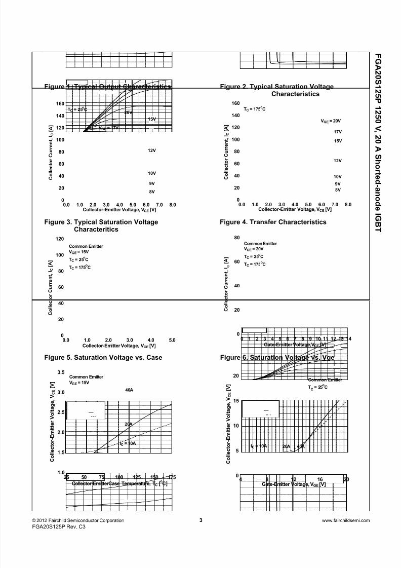
Typical Performance Characteristics
Figure 1. Typical Output Characteristics Figure 2. Typical Saturation VoltageCharacteristics
Figure 3. Typical Saturation Voltage Figure 4. Transfer CharacteristicsCharacteritics
Figure 5. Saturation Voltage vs. Case Figure 6. Saturation Voltage vs. Vge
0.0 1.0 2.0 3.0 4.0 5.0 6.0 7.0 8.00
20
40
60
80
100
120
140
160
8V
VGE = 17V
10V
9V
20VTC = 25
oC
15V
12V
C o l l e c t o r C u r r e n t , I C [ A ]
Collector-Emitter Voltage, VCE [V]0.0 1.0 2.0 3.0 4.0 5.0 6.0 7.0 8.0
0
20
40
60
80
100
120
140
160
9V
8V
17V
TC = 175oC
15V
12V
10V
VGE = 20V
C o l l e c t o r C u r r e n t , I C [ A ]
Collector-Emitter Voltage, VCE [V]
0.0 1.0 2.0 3.0 4.0 5.00
20
40
60
80
100
120
Common Emitter
VGE = 15V
TC = 25oC
TC = 175oC
C o l l e c t o
r C u r r e n t , I C
[ A ]
Collector-Emitter Voltage, VCE [V]
0 1 2 3 4 5 6 7 8 9 10 11 12 13 140
20
40
60
80Common Emitter
VCE = 20V
TC = 25oC
TC = 175oC
C o l l e c
t o r C u r r e n t , I C [ A ]
Gate-Emitter Voltage,VGE [V]
25 50 75 100 125 150 1751.0
1.5
2.0
2.5
3.0
3.5
40A
20A
IC = 10A
Common Emitter
VGE = 15V
C o l l e c t o r - E m i t t e r V o l t a g e , V
C E
[ V ]
Collector-EmitterCase Temperature, TC [oC]
4 8 12 16 200
5
10
15
20
IC = 10A 20A 40A
Common Emitter
TC
= 25oC
C o l l e c t o r - E m i t t e r V o l t a g e , V C E
[ V ]
Gate-Emitter Voltage, VGE [V]
7/30/2019 FGA20S125P
http://slidepdf.com/reader/full/fga20s125p 4/8
F GA2 0 S 1 2 5 P 1 2 5 0 V ,2 0 A S h or t e d - an
o d eI GBT
© 2012 Fairchild Semiconductor Corporation 4 www.fairchildsemi.com
FGA20S125P Rev. C3
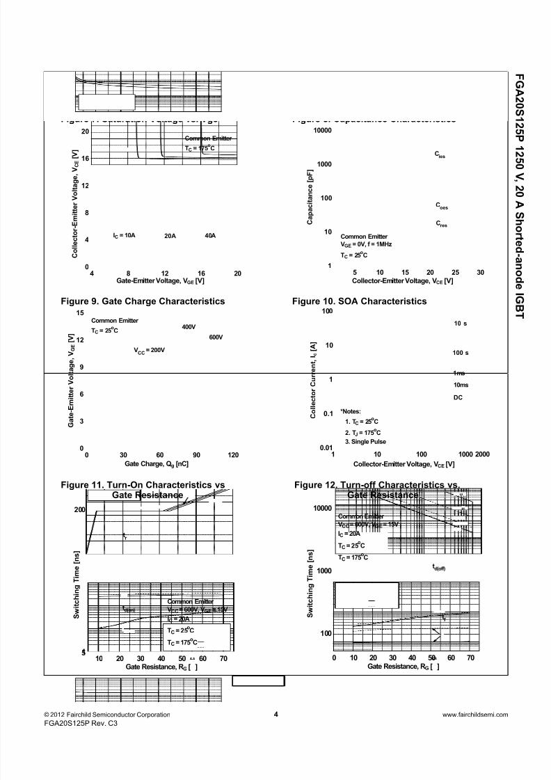
Typical Performance Characteristics
Figure 7. Saturation Voltage vs. Vge Figure 8. Capacitance Characteristics
Figure 9. Gate Charge Characteristics Figure 10. SOA Characteristics
Figure 11. Turn-On Characteristics vs Figure 12. Turn-off Characteristics vs.Gate Resistance Gate Resistance
4 8 12 16 20
0
4
8
12
16
20
IC = 10A 20A 40A
Common Emitter
TC = 175oC
C o l l e c t o r - E m i t t e r V o l t a g e ,
V C E
[ V ]
Gate-Emitter Voltage, VGE [V]5 10 15 20 25 30
1
10
100
1000
10000
Common Emitter
VGE = 0V, f = 1MHz
TC = 25oC
Cres
Coes
Cies
C a p a c i t a n c e [ p F ]
Collector-Emitter Voltage, VCE [V]
0 30 60 90 1200
3
6
9
12
15Common Emitter
TC = 25oC
600V
400V
VCC
= 200V
G a t e - E
m i t t e r V o l t a g e ,
V G E
[ V ]
Gate Charge, Qg [nC]
1 10 100 10000.01
0.1
1
10
100
2000
1ms
10ms
DC
*Notes:
1. TC = 25oC
2. TJ = 175oC
3. Single Pulse
10μs
100μs
C o l l e c t o r C u r r e n t , I c [ A ]
Collector-Emitter Voltage, VCE [V]
10 20 30 40 50 60 701
200
Common Emitter
VCC= 600V, VGE= 15V
IC = 20A
TC = 25oC
TC = 175oC
td(on)
tr
S w i t c h i n g T i m e [ n s ]
Gate Resistance, RG [Ω]
50 10 20 30 40 50 60 70
100
1000
10000Common Emitter
VCC= 600V, VGE= 15V
IC = 20A
TC = 25o
C
TC = 175oC
td(off)
tf
S w i t c h i n g T i m e [ n s ]
Gate Resistance, RG [Ω]
7/30/2019 FGA20S125P
http://slidepdf.com/reader/full/fga20s125p 5/8
F GA2 0 S 1 2 5 P 1 2 5 0 V ,2 0 A S h or t e d - an
o d eI GBT
© 2012 Fairchild Semiconductor Corporation 5 www.fairchildsemi.com
FGA20S125P Rev. C3
Typical Performance Characteristics
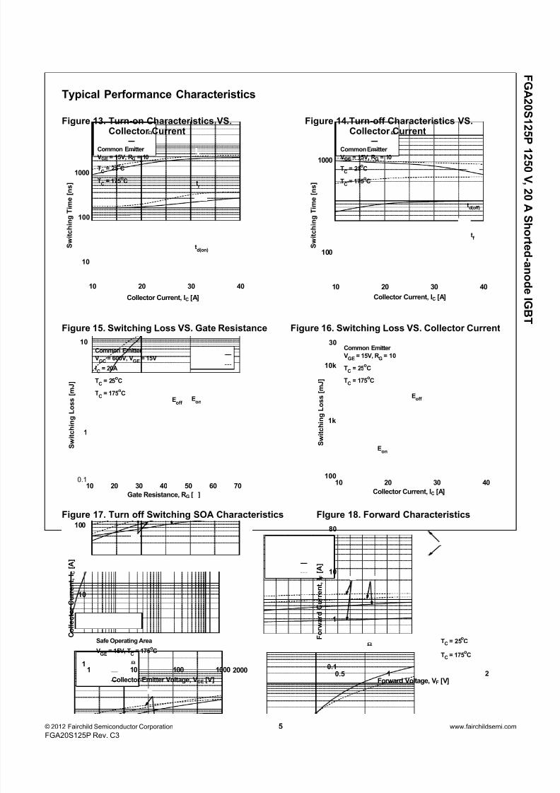
Figure 13. Turn-on Characteristics VS. Figure 14.Turn-off Characteristics VS.Collector Current Collector Current
Figure 15. Switching Loss VS. Gate Resistance Figure 16. Switching Loss VS. Collector Current
Figure 17. Turn off Switching SOA Characteristics FIgure 18. Forward Characteristics
10 20 30 40
10
100
1000
Common Emitter
VGE = 15V, RG = 10Ω
TC
= 25oC
TC
= 175oC t
r
td(on)
S w i t c h i n g T i m e [ n s ]
Collector Current, IC [A]
10 20 30 40
100
1000
Common Emitter
VGE = 15V, RG = 10Ω
TC
= 25oC
TC
= 175oC
td(off)
tf
S w i t c h i n g T i m e [ n s ]
Collector Current, IC [A]
10 20 30 40 50 60 70
1
10Common Emitter
VCC
= 600V, VGE
= 15V
IC
= 20A
TC
= 25oC
TC
= 175oC
EonE
off
S w i t c h i n g
L o s s [ m J ]
Gate Resistance, RG [Ω]
0.1 10 20 30 40100
1k
10k
Common Emitter
VGE
= 15V, RG
= 10Ω
TC
= 25oC
TC
= 175oC
Eon
Eoff
S w i t c h i n g
L o s s [ m J ]
Collector Current, IC [A]
30
1 20.1
1
10
80
TC = 25oC
TC = 175oC
Forward Voltage, VF [V]
F o r w a r d C u r r e n t , I F [ A ]
0.51 10 100 1000
1
10
100
2000
Safe Operating Area
VGE
= 15V, TC
= 175oC
C o l l e c t o r C u r r e n t , I C [ A ]
Collector-Emitter Voltage, VCE [V]
7/30/2019 FGA20S125P
http://slidepdf.com/reader/full/fga20s125p 6/8
F GA2 0 S 1 2 5 P 1 2 5 0 V ,2 0 A S h or t e d - an
o d eI GBT
© 2012 Fairchild Semiconductor Corporation 6 www.fairchildsemi.com
FGA20S125P Rev. C3
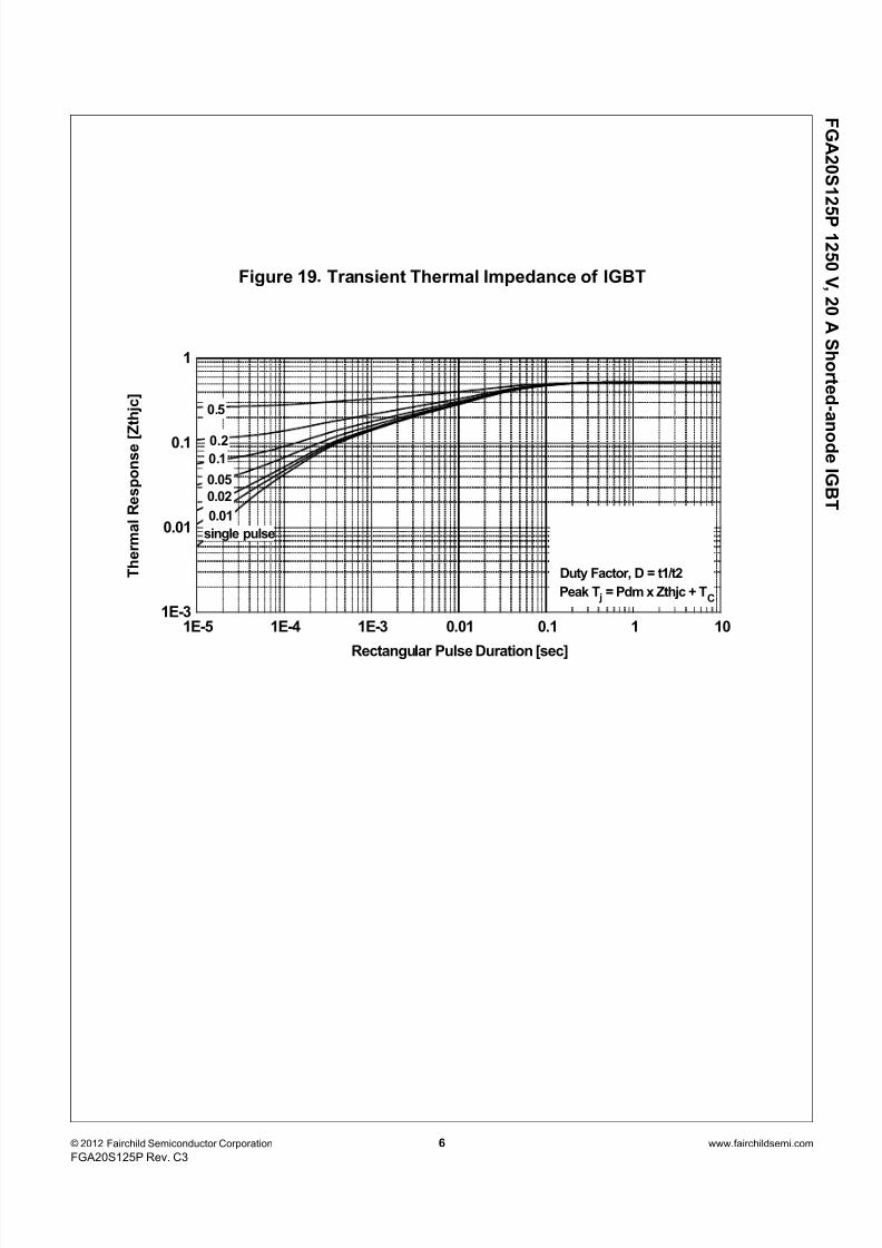
Figure 19. Transient Thermal Impedance of IGBT
1E-5 1E-4 1E-3 0.01 0.1 1 101E-3
0.01
0.1
1
0.01
0.02
0.1
0.05
0.2
single pulse
T h e r m a l R e s p o n s e [ Z t h j c ]
Rectangular Pulse Duration [sec]
Duty Factor, D = t1/t2
Peak T j = Pdm x Zthjc + TC
0.5
7/30/2019 FGA20S125P
http://slidepdf.com/reader/full/fga20s125p 7/8
F GA2 0 S 1 2 5 P 1 2 5 0 V ,2 0 A S h or t e d - an
o d eI GBT
© 2012 Fairchild Semiconductor Corporation 7 www.fairchildsemi.com
FGA20S125P Rev. C3
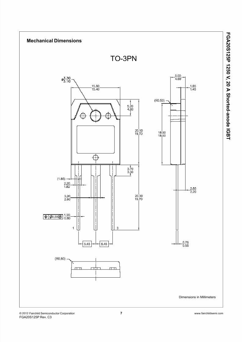
Mechanical Dimensions
TO-3PN
Dimensions in Millimeters
7/30/2019 FGA20S125P
http://slidepdf.com/reader/full/fga20s125p 8/8
F GA2 0 S 1 2 5 P
1 2 5 0 V ,2 0 A S h or t e d - an o d e
I GBT
© 2012 Fairchild Semiconductor Corporation 8 www.fairchildsemi.com
FGA20S125P Rev. C3
TRADEMARKS
The following includes registered and unregistered trademarks and service marks, owned by Fairchild Semiconductor and/or its global subsidiaries, and is not
intended to be an exhaustive list of all such trademarks.
*Trademarks of System General Corporation, used under license by Fairchild Semiconductor.
DISCLAIMERFAIRCHILD SEMICONDUCTOR RESERVES THE RIGHT TO MAKE CHANGES WITHOUT FURTHER NOTICE TO ANY PRODUCTS HEREIN TO IMPROVE
RELIABILITY, FUNCTION, OR DESIGN. FAIRCHILD DOES NOT ASSUME ANY LIABILITY ARISING OUT OF THE APPLICATION OR USE OF ANY
PRODUCT OR CIRCUIT DESCRIBED HEREIN; NEITHER DOES IT CONVEY ANY LICENSE UNDER ITS PATENT RIGHTS, NOR THE RIGHTS OF OTHERS.
THESE SPECIFICATIONS DO NOT EXPAND THE TERMS OF FAIRCHILD’S WORLDWIDE TERMS AND CONDITIONS, SPECIFICALLY THE WARRANTY
THEREIN, WHICH COVERS THESE PRODUCTS.
LIFE SUPPORT POLICY
FAIRCHILD’S PRODUCTS ARE NOT AUTHORIZED FOR USE AS CRITICAL COMPONENTS IN LIFE SUPPORT DEVICES OR SYSTEMS WITHOUT THEEXPRESS WRITTEN APPROVAL OF FAIRCHILD SEMICONDUCTOR CORPORATION.
As used here in:
1. Life support devices or systems are devices or systems which, (a) areintended for surgical implant into the body or (b) support or sustain life,and (c) whose failure to perform when properly used in accordance withinstructions for use provided in the labeling, can be reasonablyexpected to result in a significant injury of the user.
2. A critical component in any component of a life support, device, or system whose failure to perform can be reasonably expected to causethe failure of the life support device or system, or to affect its safety or effectiveness.
PRODUCT STATUS DEFINITIONSDefinition of Terms
2Cool™ AccuPower™ AX-CAP®*BitSiC™Build it Now™CorePLUS™CorePOWER™CROSSVOLT ™CTL™Current Transfer Logic™DEUXPEED®
Dual Cool™EcoSPARK®
EfficentMax™ESBC™
Fairchild®
Fairchild Semiconductor ®FACT Quiet Series™FACT®
FAST®
FastvCore™FETBench™
FPS™F-PFS™FRFET®
Global Power ResourceSM
Green Bridge™Green FPS™Green FPS™ e-Series™Gmax ™GTO™IntelliMAX™ISOPLANAR™Marking Small Speakers Sound Louder and Better™MegaBuck™MICROCOUPLER™MicroFET™MicroPak™MicroPak2™
MillerDrive™MotionMax™mWSaver™OptoHiT™OPTOLOGIC®
OPTOPLANAR®
PowerTrench®
PowerXS™Programmable Active Droop™QFET®
QS™Quiet Series™RapidConfigure™
Saving our world, 1mW/W/kW at a time™SignalWise™SmartMax™SMART START™Solutions for Your Success™SPM®
STEALTH™
SuperFET®
SuperSOT™-3SuperSOT™-6SuperSOT™-8SupreMOS®
SyncFET™
Sync-Lock™
®*
TinyBoost™TinyBuck™TinyCalc™TinyLogic®
TINYOPTO™TinyPower™TinyPWM™TinyWire™TranSiC®
TriFault Detect™TRUECURRENT®*μSerDes™
UHC®
Ultra FRFET™UniFET™VCX™VisualMax™VoltagePlus™XS™
®
™
Datasheet Identification Product Status Definition
Advance Information Formative / In DesignDatasheet contains the design specifications for product development. Specificationsmay change in any manner without notice.
Preliminary First ProductionDatasheet contains preliminary data; supplementary data will be published at a later date. Fairchild Semiconductor reserves the right to make changes at any time withoutnotice to improve design.
No Identification Needed Full ProductionDatasheet contains final specifications. Fairchild Semiconductor reserves the r ight tomake changes at any time without notice to improve the design.
Obsolete Not In ProductionDatasheet contains specifications on a product that is discontinued by FairchildSemiconductor. The datasheet is for reference information only.
ANTI-COUNTERFEITING POLICYFairchild Semiconductor Corporation’s Anti-Counterfeiting Policy. Fairchild’s Anti-Counterfeiting Policy is also stated on our external website,www.Fairchildsemi.com, under Sales Support.Counterfeiting of semiconductor parts is a growing problem in the industry. All manufactures of semiconductor products are experiencing counterfeiting of their parts. Customers who inadvertently purchase counterfeit parts experience many problems such as loss of brand reputation, substandard performance, failedapplication, and increased cost of production and manufacturing delays. Fairchild is taking strong measures to protect ourselves and our customers from theproliferation of counterfeit parts. Fairchild strongly encourages customers to purchase Fairchild parts either directly from Fairchild or from Authorized FairchildDistributors who are listed by country on our web page cited above. Products customers buy either from Fairchild directly or from Authorized FairchildDistributors are genuine parts, have full traceability, meet Fairchild’s quality standards for handing and storage and provide access to Fairchild’s full range of
up-to-date technical and product information. Fairchild and our Authorized Distributors will stand behind all warranties and will appropriately address andwarranty issues that may arise. Fairchild will not provide any warranty coverage or other assistance for parts bought from Unauthorized Sources. Fairchild iscommitted to combat this global problem and encourage our customers to do their part in stopping this practice by buying direct o r from authorized distributors.
Rev. I64
®